![]() |
![]() |
![]() |
![]() |
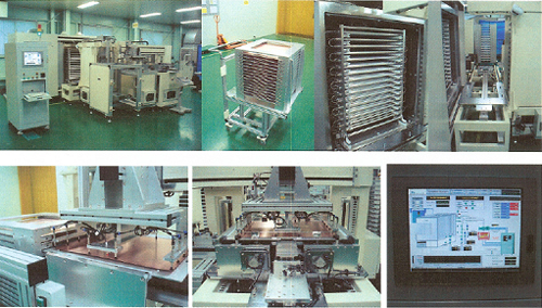
“Ultra thin PCB, VOP Board and HDI board are too thin to be dealt with humans so there is high risk of defect by human mistake or error.
To reduce this kind of mistake due to handling errors, fully automated system is required which can ensure all the process from loading to unloading is automated.
Full Auto plasma system should be designed by considering characteristics of PCB such as size, handling method, line arrangement etc”
![]() |
![]() |
![]() |
![]() |
You must be logged in to post a comment.
Manufacturer: First EIE, Switzerland Photo Plotter
Manufacturer: Hitachi, JapanPWB Co2 Laser Drilling Machine
Manufacturer: Kuang Chien Computer Co., Ltd. (Comweb, Taiwan)PCB Fixture Driling / Routing Machine Model No. : CRD-520
Manufacturer: Hakuto Co. Ltd., JapanLaminator
Manufacturer: Hakuto Co. Ltd., Japan Automatic Exposure System(Model : HAP5020)
The newly developed image Processing Technology gives highly reliable detection of OPEN, SHORT, CONTAMINATION, STAIN, SCRATCH, and DISCOLORATION on PCBs. Miss-Detection by Over Care is minimized. The most suitable for inspection on High Density Board such as COB and BGA,and inspection on solder leveler PCBs
Manufacturer: Hitachi, Japan PWB Hole Analyzer / PWB Hole Tester Machine

There are no reviews yet.