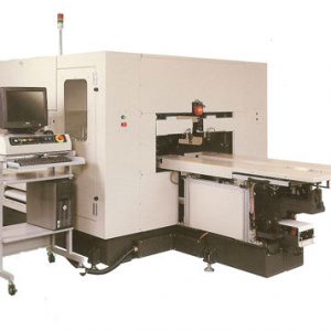
Manufacturer: First EIE, Switzerland Photo Plotter
Be the first to review “Photo Plotting” Cancel reply
You must be logged in to post a comment.
related items
PANEL and PATTERN as well as automatic panel loading and collecting devices.For processing thin panels and panels with tiny holes, PAT takes special measures to do the loading and bubble removal in order to improve yields.
An even or no trace matte finish appeared by the abrasive spray is the best condition of the panel surface for the pre-treatment of D/F lamination, solder mask and liquid photo resist.
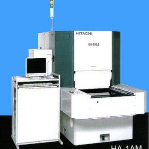
Maskless, Beam – overlapping method. Applicable to next generation PWB processes
Hitachi original high – speed RIP (SRC) and light source provide long – lasting uniform light intensity and are capable of high – precision exposure
This high performance multilayer press was designed for PCB labs to enable quick prototyping of multilayer PCBs of up to 6 or 8 layers according to industry standards. A compact and floor standing aluminium rack contains all parts of the unit including pressure supply, press plates and heaters.
This line is to form the patterns on the panels by chemical treatment, whose configuration is Developing + Etching + Stripping. Developing and Etching module with our rotary spray system are readily achievable high etching factor to a fine pattern. It can be used a chemical, CuCl2 and FeCl2.\
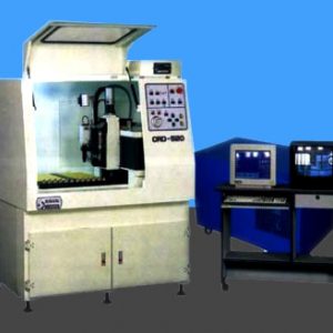
Manufacturer: Kuang Chien Computer Co., Ltd. (Comweb, Taiwan)PCB Fixture Driling / Routing Machine Model No. : CRD-520
The name IONEX stands for ION Exchanger, which is the very heart of this modern waste water treatment system. In total it consists of a two-stage filtration, two ion-exchange and one PH-leveling units. IONEX is ideally suited for all waste water cleaning processes in modern PCB prototype laboratories.
Manufacturer: Hitachi, Japan PWB Hole Analyzer / PWB Hole Tester Machine


There are no reviews yet.